 jessica@honch-etech.com
 English

 Item(s)

12 layer HBM4 production has been delivered!
The HBM4 delivered this time is SK Hynix's first product to be delivered to Nvidia in final specifications, and has completed the quality certification of Nvidia's next-generation AI platform Vera Rubin.
It is reported that SK Hynix will further expand the shipment scale of HBM4 from September this year to meet the supply demand of Nvidia's high-end AI computing chips.

HBM, That is, high bandwidth memory, which is a vertically stacked DRAM. Usually, it is tightly connected to GPUs and AI accelerators through silicon intermediaries or advanced packaging methods, providing much higher bandwidth than traditional server memory.
Simply put, GPU is responsible for computation, while HBM is responsible for feeding data to GPU at high speed.
HBM will continue to iterate, with each generation upgrading around higher bandwidth, larger capacity, and lower power consumption.
Currently, HBM3E is widely used on mainstream AI platforms, mainly serving Nvidia Blackwell series GPUs.
Taking the 12 layer HBM3E as an example, the maximum single capacity can reach 36GB, the single pin transmission speed is about 9.2Gbps to 9.8Gbps, and the single stack bandwidth can reach about 1.2TB/s to 1.28TB/s.
And HBM4 is aimed at the next generation of AI platforms, especially the NVIDIA Vera Rubin architecture.

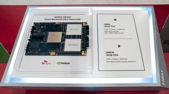
Compared with the previous generation, one of the biggest changes of HBM4 is the increase in I/O count to 2048, wider data channels, and doubled bandwidth.
SK Hynix previously stated that the energy efficiency of HBM4 has increased by over 40% compared to the previous generation, and the highest AI service performance can be improved by about 69% after application.
Meanwhile, the SK Hynix HBM4 has a running speed of over 10Gbps, significantly higher than the JEDEC standard of 8Gbps.
From a platform perspective, the Nvidia Vera Rubin GPU is expected to carry up to 288GB of HBM4 memory; The AMD Instinct MI455 is expected to be equipped with higher capacity, up to 432GB.
At the same time, SK Hynix is also expanding its next-generation DRAM production capacity.

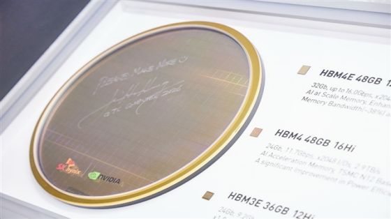
SK Hynix plans to advance the production of Phase Y1 from the originally scheduled May next year to February next year. The company will start building a trial production line from February next year and carry out large-scale equipment installation from March to April.
The goal of this wafer fab is to produce the sixth generation 10 nanometer level 1c DRAM. The related products will be used for AI server DDR and LPDDR products, and are planned to serve the next generation HBM4E.
Related Information





- 1500+ Daily average RFQ Volume

- 20,000.000 Standard Product Unit

- 1800+ Worldwide Manufacturers

- 15,000+ In-stock Warehouse


